DESHIMA
A short overview of the DESHIMA spectrometer, the optical chain and the physics behind the detectors
In 2017, as part of the first light campaign, the first DESHIMA device was proven to work as expected when mounted to the ASTE telescope[1], but was limited in scope. The chip had just 49 channels and a spectral resolution of $\nu/\Delta \nu\approx380$, with a spectral range of $327\:\mathrm{GHz}$ to $377\:\mathrm{GHz}$. This proof of concept led to the development of DESHIMA 2.0 and the Science Verification Campaign[2]. With 347 channels in the range of $220\:\mathrm{GHz}$ to $440\:\mathrm{GHz}$ and a spectral resolution of $\nu/\Delta \nu\approx500$, DESHIMA 2.0 is much more capable. Besides the obvious bandwidth and channel upgrades, the sensitivity has also been increased four to eight fold [3]. In this thesis I will be discussing DESHIMA 2.0, but it is entirely applicable to any DESHIMA-type spectrometer.
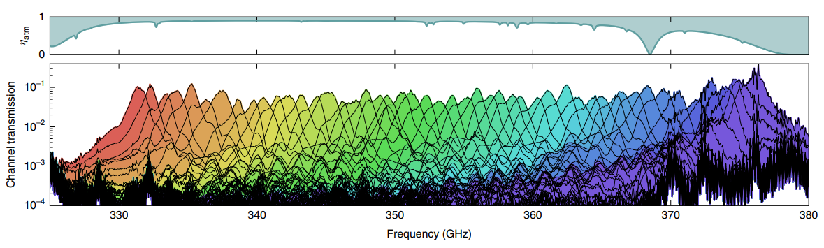 The 49 filter channels and their transmission as measured from the original DESHIMA. Image taken from [1]
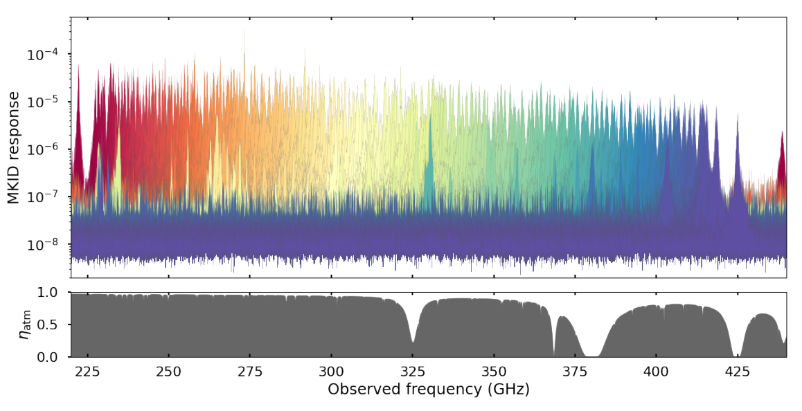 The 347 filter channels and their transmission as measured on DESHIMA 2.0. Image taken from [2]
The Optical Chain
As mentioned, DESHIMA is installed on the ASTE radio-telescope in the Atacama desert. This means that the light from distant galaxies travels through the atmosphere towards the dish of the telescope, where it gets reflected to the secondary mirror. The set of primary and secondary mirror is called a Cassegrain reflector and focuses the signal.
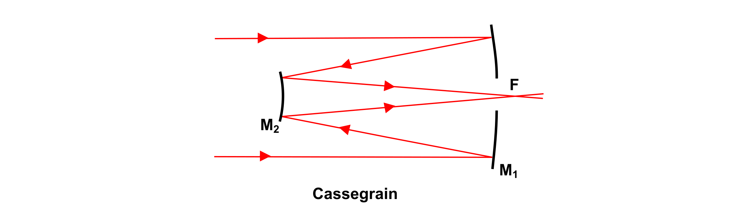 A schematic drawing of a Cassegrain reflector. Image taken from [4]
After the incoming signal has been focused, it passes a set of mirrors in the telescope cabin and then passes through a window into the cryostat. At a temperature of $4\:\mathrm{K}$ the light passes through a low-pass filter, a third set of mirrors and a polarizer, until reaching the spectrometer chip at a temperature of $120\:\mathrm{mK}$.
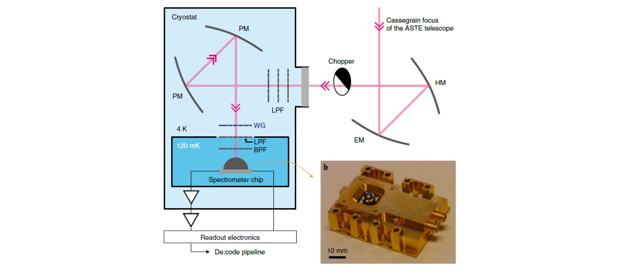 The optical chain of the DESHIMA 1.0 spectrometer. After passing through the Cassegrain reflector, the light hits an ellipsoidal mirror (EM), a hyperbolic mirror (HM), a low-pass filter (LPF), two parabolic mirrors (PM), a wire grid polarizer (WG) a low pass and band pass filter (LPF, BPF) until it hits the spectrometer. DESHIMA 2.0 has too wide a range to use the band pass filter, so it is omitted. Image taken from [1]
Every optical component has a corresponding efficiency $\eta_\mathrm{opt}$ and transmits only a part of the incoming signal $\mathrm{PSD_{in}}$ while also adding to that signal its own emission $\mathrm{PSD_{opt}}$, in a process called a radiative transfer[5]:
$$\begin{equation} \mathrm{PSD_{out}}=\eta_\mathrm{opt}\mathrm{PSD_{in}} + \left(1-\eta_\mathrm{opt}\right)\mathrm{PSD_{opt}} \end{equation}$$Here $\mathrm{PSD}$ is the power spectral density expressed in units of $\mathrm{[WHz^{-1}]}$, which for the emission of the optical component is given by Johnson-Nyquist[6]:
$$\begin{equation} \mathrm{PSD_{opt}}\left(\nu,T\right)=\frac{h\nu}{e^{h\nu/k_BT}-1} \end{equation}$$which depends on both temperature and frequency. Therefore the radiative transfer of the optical chain needs to be calculated across the frequency spectrum for every component at its temperature. This means that the total optical chain is a series of radiative transfers. For a simple two mirror system this is the following $$\begin{equation} \mathrm{PSD_{in}}\rightarrow\mathrm{M1}\rightarrow\mathrm{PSD_{intermediate}}\rightarrow\mathrm{M2}\rightarrow\mathrm{PSD_{out}} \end{equation}$$
To simplify the calculations, efficiencies of components at the same temperature can be taken together
$$\begin{equation} \begin{split} \mathrm{PSD_{out}}&=\eta_2\mathrm{PSD_{intermediate}} + \left(1-\eta_2\right)\mathrm{PSD_{opt}}\\ &=\eta_2\left(\eta_1\mathrm{PSD_{in}} + \left(1-\eta_\mathrm{opt}\right)\mathrm{PSD_{opt}}\right) + \left(1-\eta_\mathrm{2}\right)\mathrm{PSD_{opt}}\\ &=\eta_1\eta_2\mathrm{PSD_{in}}+\eta_2\left(1-\eta_1\right)\mathrm{PSD_{opt}}+\left(1-\eta_2\right)\mathrm{PSD_{opt}}\\ &=\eta_1\eta_2\mathrm{PSD_{in}}+\eta_2\mathrm{PSD_{opt}}-\eta_1\eta_2\mathrm{PSD_{opt}}-\eta_2\mathrm{PSD_{opt}}+\mathrm{PSD_{opt}}\\ &=\eta_1\eta2\mathrm{PSD_{in}} + \left(1-\eta_1\eta2\right)\mathrm{PSD_{opt}} \end{split} \end{equation}$$At ASTE, the atmosphere is around $273\:\mathrm{K}$ and the cabin is $290\:\mathrm{K}$. as mentioned before the cold optics and the chip are $4\:\mathrm{K}$ and $120\:\mathrm{mK}$ respectively. If we plot the $\mathrm{PSD_{opt}}$ for the different components along with the power a galaxy transmits to a telescope dish with a diameter of $10\:\mathrm{m}$, we get the following figure:
Besides the PSD emitted by the chip, the optical components are much brighter than the astronomical source. Take note that the atmosphere and the cabin are almost at the same temperature and therefore have almost the same PSD.
As is clear from the figure, the efficiency of all but the chip really matter in the range DESHIMA measures in, which is why they need to be modeled carefully in deshima-sensitivity. In order to look at the amount of loading these sections impart on the detector, we can look at the effective power spectral density $\mathrm{PSD_{opt,eff}}$:
with $\eta_i$ the efficiencies of the optical components in the part of the chain that is at the same temperature.
The effective loading from the various optical components. Take note that the simulated galaxy source is still not attenuated
Because of the faintness of a typical source, everything but the chip is still brighter than the source, while the latter is not even attenuated. From the radiative transfer we have seen that with every optical component the source loses some of its power due to the efficiency of these components, so in actuality the source at the detector would be even less bright.
The Filterbank
After the optical chain the light is passed to a filterbank containing 347 bandpass filters, with constant spectral resolution $R=\nu/\Delta_\nu=500$ and a center frequency for the $i$th filter given by [7]:
$$\begin{equation} \nu_i=\nu_\mathrm{min}\left(1+\frac{1}{R}\right)^i \end{equation}$$with $\nu_\mathrm{min}=220\:\mathrm{GHz}$[3]. This expression ensures that the filter channels are spaced such that the bandwidths of each filters are right next to each other without overlapping, since a constant spectral resolution means the bandwidths get progressively wider as the center frequencies increase.
Due to their spatial efficiency the signal is bandpass filtered by resonators with a Lorentzian pass band[7]. In the figures below a schematic overview of a filter is given and the transmission parameters of this filter are shown.
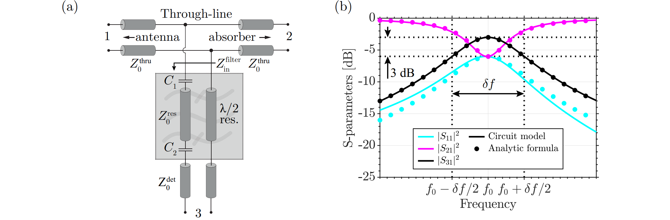 a) A schematic viewing of the filter design. Port 3 is towards the detector. b) The S-parameters of the filter transmission. Here S31 is the transmission parameter from the filter input to the detector. Here the solid lines are the simulated circuit and the dots are the analytical approximations. Note the 3dB cutoff point at the bandwidth for the S31 transmission. Images taken from [7]
The transmission from the input to the detector through the filter is given by $\left|S_{31}\right|^2$. From [7] we get an approximation for $S_{31}$ around the center frequency of the filter $v_0$ as:
$$\begin{equation} S_{31}\left(\nu\right)\approx\frac{S_{31}\left(\nu_0\right)}{1+j2Q_l\frac{\nu-\nu_0}{\nu_0}} \end{equation}$$With $j$ the imaginary unit and $Q_l$ the loaded quality factor. This approximation is marked with black dots in the figure above.
In a resonant circuit the quality factor $Q$ is defined as[8]:
$$\begin{equation} Q=\frac{\nu_0}{\Delta\nu} \end{equation}$$Therefore, the transmission $\left|S_{31}\right|^2$ is given as:
$$\begin{equation} \left|S_{31}\left(\nu\right)\right|^2 \approx \frac{\left|S_{31}\left(\nu_0\right)\right|^2}{1+4Q_l^2\left(\frac{\nu-\nu_0}{\nu_0}\right)^2}=\frac{\left|S_{31}\left(\nu_0\right)\right|^2}{1+4\left(\frac{\nu-\nu_0}{\Delta\nu}\right)^2}=\frac{\left|S_{31}\left(\nu_0\right)\right|^2}{1+\left(\frac{\nu-\nu_0}{\gamma}\right)^2} \end{equation}$$with $\gamma=\Delta\nu/2$. This equation describes a Lorentzian with $\gamma$ being the half maximum at half width and $\left|S_{31}\left(\nu_0\right)\right|^2$ the peak value at $\nu=\nu_0$. As the figure also shows the resonance is tuned such that the bandwidth $\Delta\nu$ is the same as the full width at half maximum. In other words the transmission within the bandwidth is always greater or equal to $50\%$ the peak transmission at the resonance frequency.
Situated after each of these 347 filter channels is a detector to detect the bandpassed signal.
The Detectors
DESHIMA detects photons using (Microwave) Kinetic Inductance Detectors, or (M)KID for short. These work by exploiting the energy gap in superconductors.
Inside the superconductor electrons are coupled together in Cooper-pairs at energy levels $E_F$. When these pairs get excited, the electrons move as quasiparticles to a higher energy level $E\ge E_F+\Delta_\mathrm{Al}$ [9], where $\Delta_\mathrm{Al}=188\:\mathrm{meV}$ the gap energy of an aluminium superconductor[5].
Therefore, if an incoming photon carries enough energy to excite a pair of these electrons, specifically more than $2\Delta_\mathrm{Al}$, it increases the number of quasiparticles. This means that the photon needs
$$\begin{equation} E=h\nu\gt2\Delta_\mathrm{Al}\iff \nu\ge \frac{2\Delta_\mathrm{Al}}{h}\approx 91\:\mathrm{GHz} \end{equation}$$which is perfect for the $220\:\mathrm{GHz}$ to $440\:\mathrm{GHz}$ range we are interested in.

When an incident photon has enough energy to overcome the energy gap, the cooper pair breaks and generates quasiparticles. Image taken from [9]
Resonance Circuit
The cooper pairs decrease the inductance[10], so when these are broken the overall inductance increases. In order to measure this change in inductance, the detector is designed as parallel sets of RLC circuits, designed such that the total frequency of the resonance is in the range of $4-6\:\mathrm{GHz}$[2].
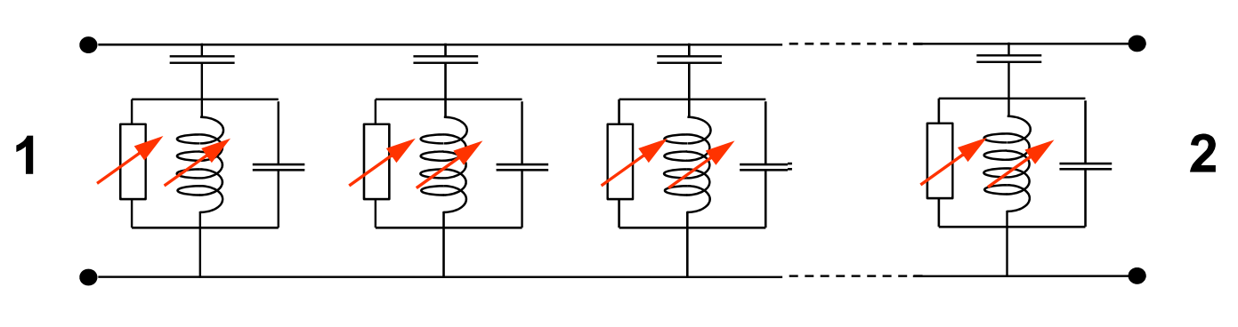
RLC circuits are used to read the change in inductance. Parallel RLC circuits divide the frequency to a range that the read-out electronics can handle. Image taken from [9]
These circuits are resonant when the reactance of the inductor and the capacitor are equal:
$$\begin{equation} X_L=X_C\iff\omega L = \frac{1}{\omega C}\iff\omega_r=\frac{1}{\sqrt{LC}} \end{equation}$$and therefore the resonance gets lowered by a decrease in cooper pairs.
In order to read out the detector, a signal at the resonant frequency is fed into the superconductor. When the resonant frequency decreases, so does the transmission and therefore an increase in power is measured[9].

The change in resonance frequency lowers the transmission, therefore increasing the power. This increase in power is measured. Image taken from [9]
Bibliography
- [1]A. Endo et al., “First light demonstration of the integrated superconducting spectrometer,” Nature Astronomy, vol. 3, no. 11, pp. 989–996, 2019, doi: 10.1038/s41550-019-0850-8.
- [2]A. Taniguchi et al., “DESHIMA 2.0: development of an integrated superconducting spectrometer for science-grade astronomical observations.” 2021.
- [3]M. Rybak et al., “DESHIMA 2.0: Rapid redshift surveys and multi-line spectroscopy of dusty galaxies.” 2021.
- [4]H. Hahn, “Diagram Reflector Cassegrain.” Wikimedia, 01-Apr-2010 [Online]. Available at: https://nl.m.wikipedia.org/wiki/Bestand:Diagram_Reflector_Cassegrain.svg
- [5]A. Endo and A. Taniguchi, “deshima-sensitivity v0.3.0,” pypi.org. Open Source, Jun-2021 [Online]. Available at: https://pypi.org/project/deshima-sensitivity/
- [6]A. Endo, “Session 4 | Photon Noise,” EE3350TU Introduction to Radio Astronomy. Dec-2020.
- [7]A. P. Laguna, K. Karatsu, D. Thoen, B. Murugesan rp, A. Endo, and J. Baselmans, “Terahertz Band-Pass Filters for Wideband Superconducting On-Chip Filter-Bank Spectrometers,” IEEE Transactions on Terahertz Science and Technology, vol. 11, no. 6, pp. 635–646, 2021, doi: 10.1109/tthz.2021.3095429.
- [8]C. K. Alexander and M. N. Sadiku, Fundamentals of Electric Circuits, 7th ed. McGraw-Hill Education, 2021.
- [9]J. Baselmans, “Kinetic inductance detectors,” Journal of Low Temperature Physics, vol. 167, no. 3-4, pp. 292–304, 2012, doi: 10.1007/s10909-011-0448-8.
- [10]R. Meservey and P. M. Tedrow, “Measurements of the Kinetic Inductance of Superconducting Linear Structures,” Journal of Applied Physics, vol. 40, no. 5, pp. 2028–2034, 1969, doi: 10.1063/1.1657905.